Discrete logic chips VGA video card
February 17, 2021
The next step in my discrete logic computer project after designing a CPU and building a new ALU is to build a video card.
Here’s what it can do:
Video card parameters #
I chose to implement a 80x30 text mode with 4 bit color (like in EGA) because of the address space limitations (only up to 216 bytes can be addressed by my CPU, video buffer should not take a significant part of that). Also I like the look of old-school text modes and the EGA colors.
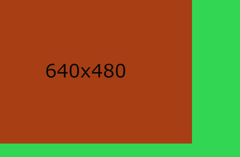
The 80x30 8x16 characters make a 640x480 pixel image, which is the industry standard VGA resolution and must be supported by all monitors.
Video signal #
There is plenty of information in the Internet describing the VGA timings. For example, this page or this page. In short, you need to count rows and columns and depending on the counter values toggle the VSYNC and HSYNC signals or output the analog color signals.
What I haven’t found anywhere is what phase should VSYNC signal have relative to HSYNC. Should VSYNC pulse start at the beginning of the HSYNC pulse as on the diagram below?

Or should it start on HSYNC pulse end?
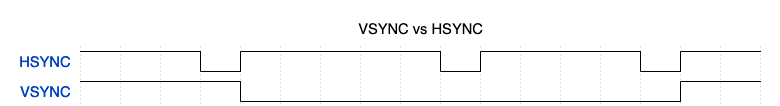
Maybe this doesn’t matter at all? I suspect this is the case. My implementation generates VSYNC as shown on the first diagram and it works fine with the monitor I have.
So, first of all, for my video card I needed two counters: row and column. Then I needed a logic to provide HSYNC and VSYNC and to reset the counters when they reach the maximum value (800 for column and 525 for row - the numbers from the VGA standard). The column counter should count at 25.175 MHz (the pixel clock frequency from the VGA standard).
If, instead of hardware, this would be implemented in software, signal generation would look something like that:
for vy in range(525):
    vsync = ~((vy >= 480 + 10) & (vy < 480 + 10 + 2))
    for hx in range(800):
        hsync = ~((hx >= 640 + 16) & (hx < 640 + 16 + 96))
I needed to implement those complex expressions using boolean functions from the list. Let’s see how it can be done for vsync. vsync is zero when the counter value is between 490 and 492. This is equivalent to the following condition:
vsync = ~(vy == 490 | vy == 491)
The counter counts up to 525, this means we need 10 bits. Now let’s rewrite the condition using binary numbers:
vsync = ~(vy == 01 1110 1010 | vy == 01 1110 1011)
Both constants only differ in the lowest bit. This means, the bit 0 of vy doesn’t take part in the condition: we don’t care about its value. Let’s write x instead of that bit:
vsync = ~(vy == 01 1110 101x)
Quite a bit simplier already.
When vsync is 1? If bits 2, 4 or 9 of vy are ones, vsync should be one. If any of bits 1, 3, 5, 6, 7, or 8 is zero, vsync should be one too. Let’s write this:
vsync = vy[2] | vy[4] | vy[9] | ~(vy[1] & vy[3] & vy[5] & vy[6] & vy[7] & vy[8])
Looks scary. But we can remember that vy cannot be greater than 524 (10 0000 1100 binary). This means, vy can’t be something like 11 1110 1010 (bits 5 to 9 all ones). If bit 9 is one, bits 5 to 8 will be zero. This lets us to exclude vy[9] from the condition - this case will be already covered by the expression in brackets:
vsync = vy[2] | vy[4] | ~(vy[1] & vy[3] & vy[5] & vy[6] & vy[7] & vy[8])
Now let’s pick the largest available logical functions from the list. We can use 74LV21A - 4 input AND, 74LV10A - 3 input NAND and 74LV32A - two input OR. The condition is implemented with four gates:
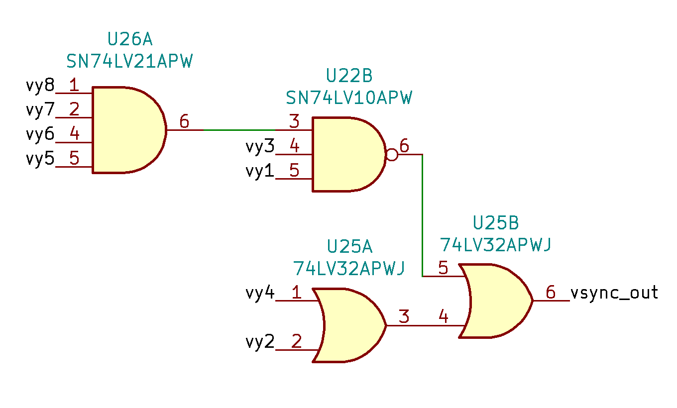
Image generation #
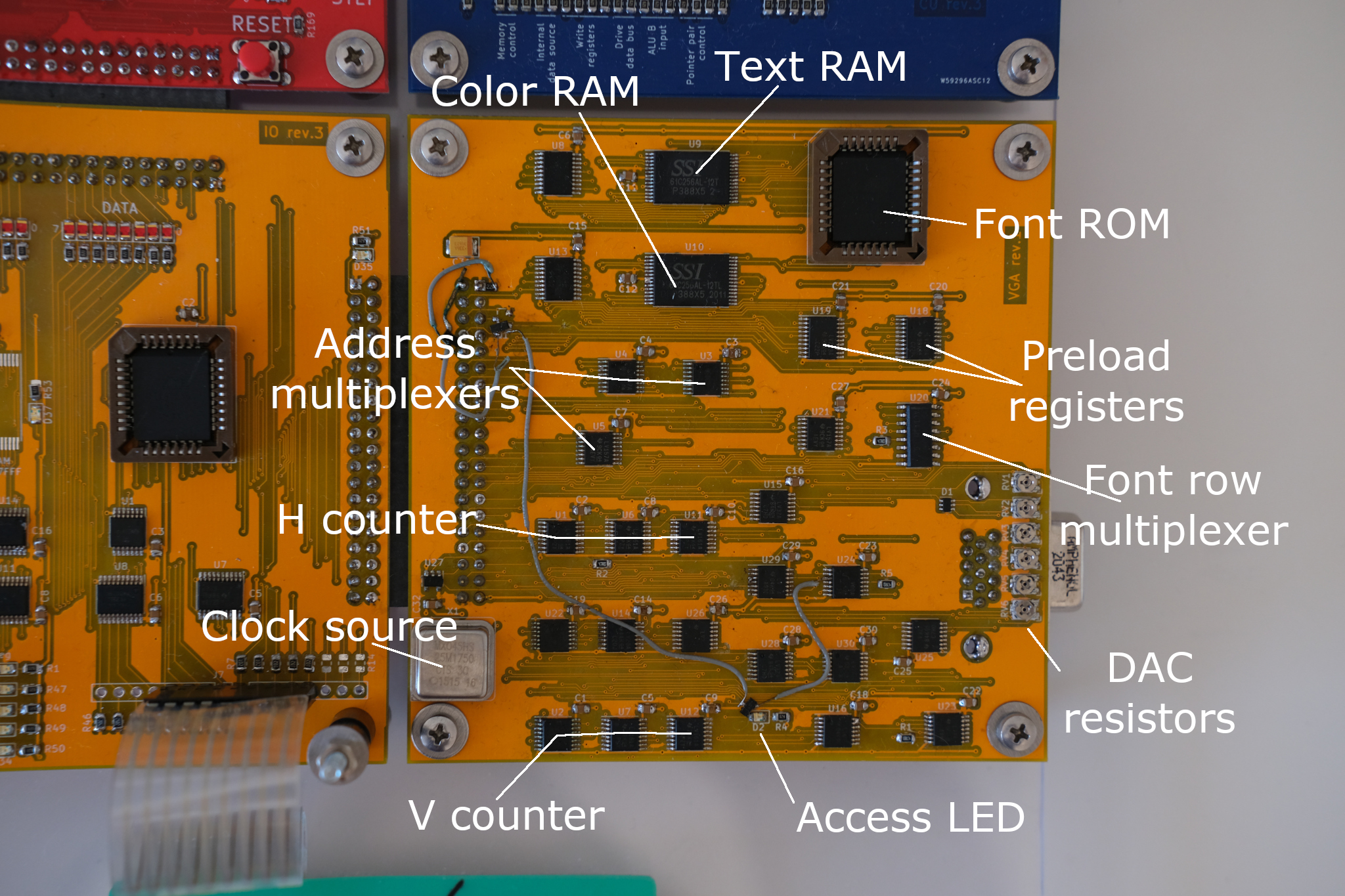
The generic character generator is shown below.

Upper bits of row and column counters are combined into RAM index. Character is then loaded from the text RAM. Then the character code and lower row bits are combined and fed into the CGROM (character generator ROM) which contains font data. The font row (8 bit) is loaded from the ROM. Then, using a multiplexer, a single bit is selected from the font row. This bit is then used to select the color (foreground or background) from the color pair which was loaded from the color RAM.
Unfortunately, this doesn’t work. One pixel lasts for about 40 nS (pixel clock is 25.175 MHz), 8 pixels - 320 nS. The ROM access time for AT28C256 is 150 nS. This means that when everything is loaded, almost half of the character will already be displayed using intermediate rubbish from the ROM.
Fortunately, total access time is less than single character display time. This means, we can implement a pipeline and preload font data while previous character is still displayed.
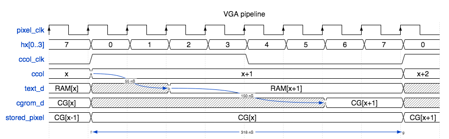
To implement this pipeline, I added two registers (74LV273A) to hold color and font row. They are controlled by a dedicated clock signal, which is essentially an inversed hx[2].

Now character output is delayed by 8 pixels. HSYNC needs to be adjusted, otherwise the timings will be incorrect. The easiest way to do it is to buffer it the same way color and font are buffered. I use a flip-flop 74LV74A to delay HSYNC.
Color DAC #
The pixel pipeline outputs a 4-bit color in an IRGB format, where ‘I’ stands for intensity. VGA accepts analog signals. The circuit to convert digital signals to analog is pretty simple:
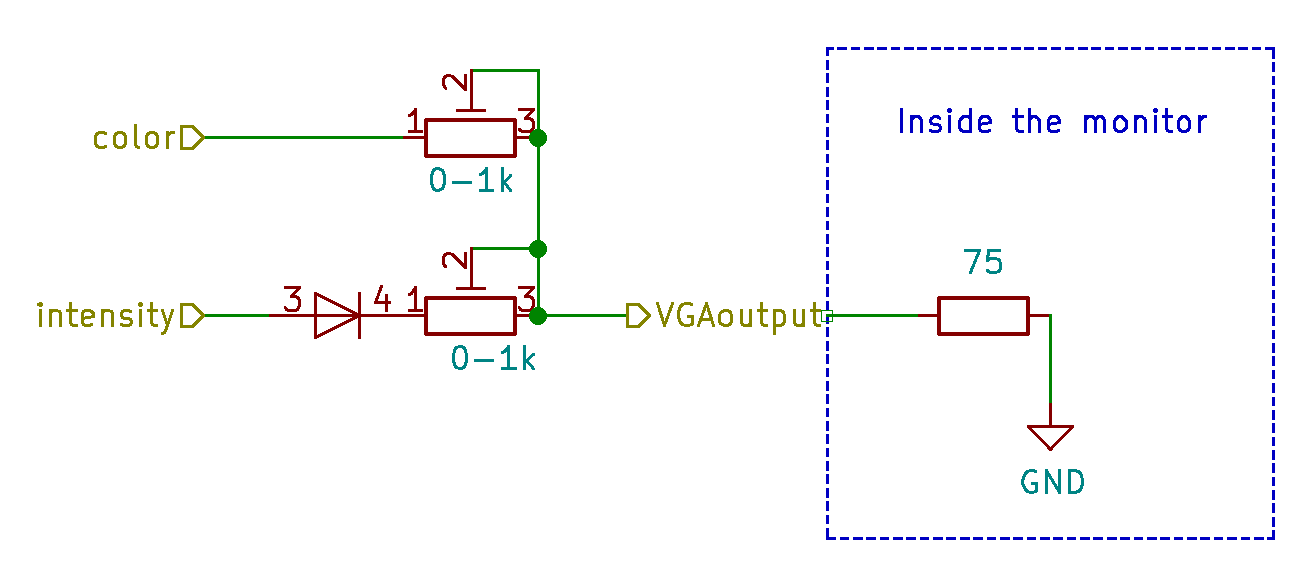
You just need two resistors and a diode for each channel. The diode is there because the single intensity signal is used for all three color channels. Diode prevents interference between channels through the intensity line. I used trim potentiometers to make sure the VGA voltages are correct regardless of diode parameters and digital chips output voltage.
Memory access #
CPU needs to write data into video memory. Fortunately, there’s plenty of time to do that:
This picture is a 800x525 pixel image which shows visible area (in brown) inside a VGA frame. Inside the brown area the text and color RAM address is taken from the counters as shown before. Inside the green area memory address is taken from the CPU address bus. This address multiplexing is done by three 74LV157A chips.
When pixel counter is inside the brown area, CPU must stop and wait if it needs to access the video buffer. I had a lot of adventures with implementing this mechanism.
First of all, I made a mistake in the VGA board: the RDY signal was falsely asserted even if the video buffer wasn’t accessed. I had to cut some tracks and hand-wire the correct logic using some transistors.
In my first implementation the CPU wasn’t capable of waiting for a peripheral device. I simply didn’t need it in the basic system. When I built the video card, I needed to modify the CPU to support this signal. My first implementation was to change the control unit in a way that when executing a load or store instruction, the memory operation will be delayed until the RDY signal is released.
But it didn’t work out. I won’t describe it in details here, but that solution was too complex, some corner cases weren’t covered. As a workaround, when I needed to write a value into video buffer, I just called the ST instruction 20 times. 20 instructions at 1.75 MHz covered one VGA scan line: at least one of the writes was successfull, and the value was written correctly.
Then I implemented the RDY in a different way: the RDY signal now goes directly to the clock generator and stops the clock if asserted. Since the clock generator is on the registers module, I had to make a new revision of that board. This way waiting for memory works flawlessly.
From the programmer’s point of view, the text and color buffers take 4 kB each starting at the addresses 0xE000 and 0xD000 respectively. Unlike IBM EGA/VGA, where characters and colors are interleaved in memory, my video card uses separate segments. It was easier to implement and to program: the text buffer is flat, you can just copy strings there as they are without any need to mix the color between characters.
The result #
Here’s what the VGA board looks like:
And the whole system with new registers, IO and control modules:
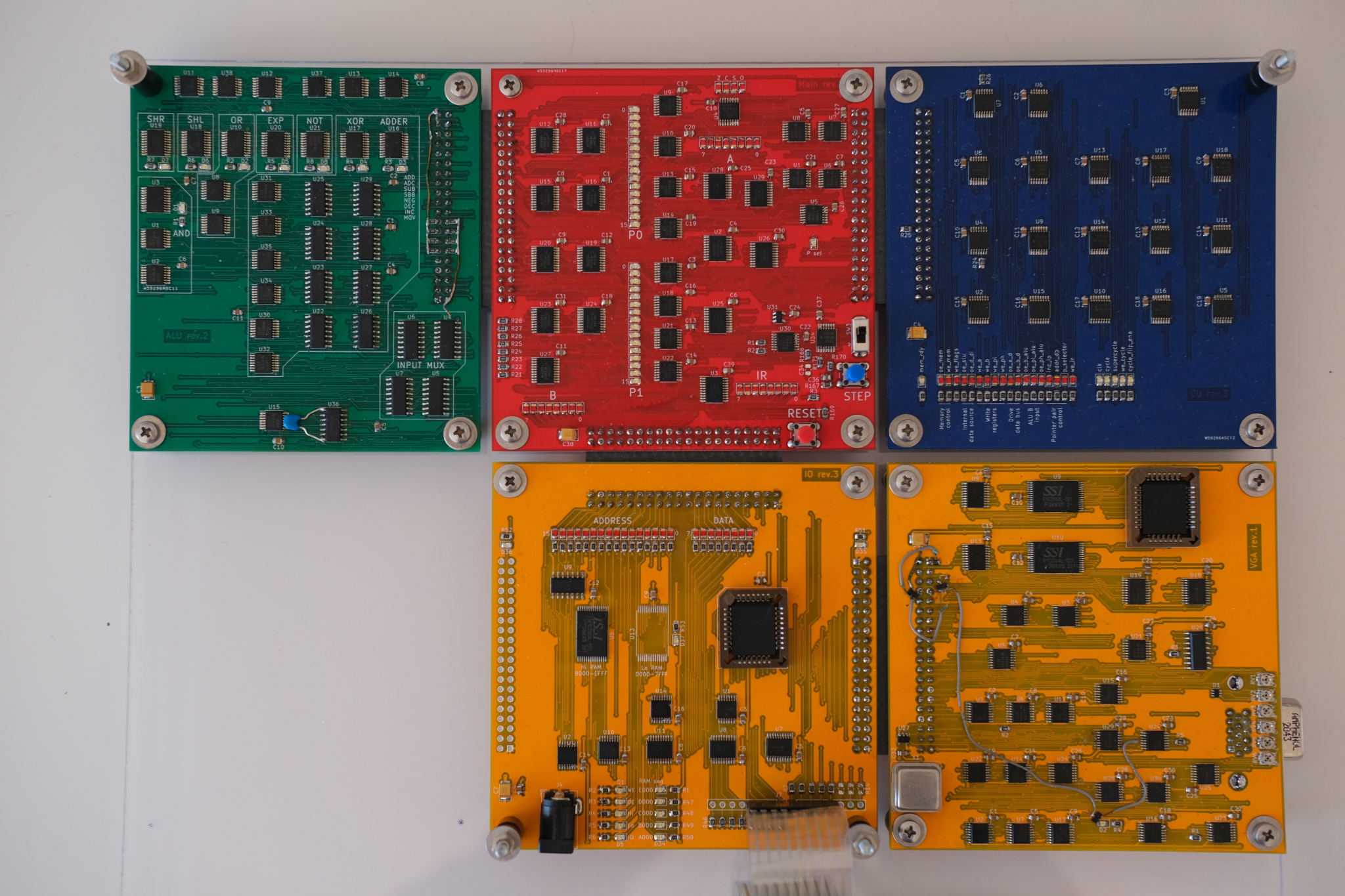
No board on this picture is from the original post, everything is new.
I needed a new IO module to support side board connections. Also, I’ve implemented a register to switch between ROM and RAM, if I want to load some programs dynamically in the future. There’s no need in the LCD module anymore, so I removed it.
And one more video: Conway’s game of Life. The square “pixels” are in fact characters (code 220 from CP437).
Amateur discoveries #
I’m a software guy, I’ve never studied electrical engineering at a university. During this project I made some discoveries which may seem obvious to professionals, but for me they were new.
When I started testing the video card, the video signal was sometimes unstable. More than that, sometimes the whole system behaved strangely, like if it was reset at some point. The weird behavior happened if I ran certain programs, but with other programs everything was totally fine. After sitting with an oscilloscope for a while, I’ve cornered the problem: address bus signals sometimes caused interference on the reset line because the tracks were too close on the board. This was my first encounter of crosstalk.
It turned out that the use of 74AC series in the CPU was a big mistake. That logic family is so fast that rapid raise and fall times of the signals caused all kinds of interference. It looks like a miracle that everything worked fine with 74AC up until now. In the video card I used the other series, 74LV-A, which is equally fast, but makes less noise. However, I couldn’t notice any difference on my oscilloscope.
To fix the crosstalk problem, I had to cut the reset track which goes to the pixel counters. After doing that, the problem disappeared.
When I remade the registers module to support RDY, I used the classic 74HC series. They aren’t as fast as 74AC or 74LV-A, but the output signals are nice and smooth. Now, after I’ve made all those amendments, my system runs smoothly at 3.5 MHz.