Discrete logic network card
April 9, 2024
This post is a continuation of my journey to build a complete computer system using discrete logic components. At this point I have made a computer capable of running network applications like an HTTP server or a LAN game.
Last year I built a physical level adapter which converts a 10BASE-T Ethernet signal to SPI and back. Back then I used an STM32 microcontroller to test its operation, now I’m implementing a MAC layer module to connect it to my homebrew computer.
Both adapters are full-duplex and have independent transmitter and receiver parts.
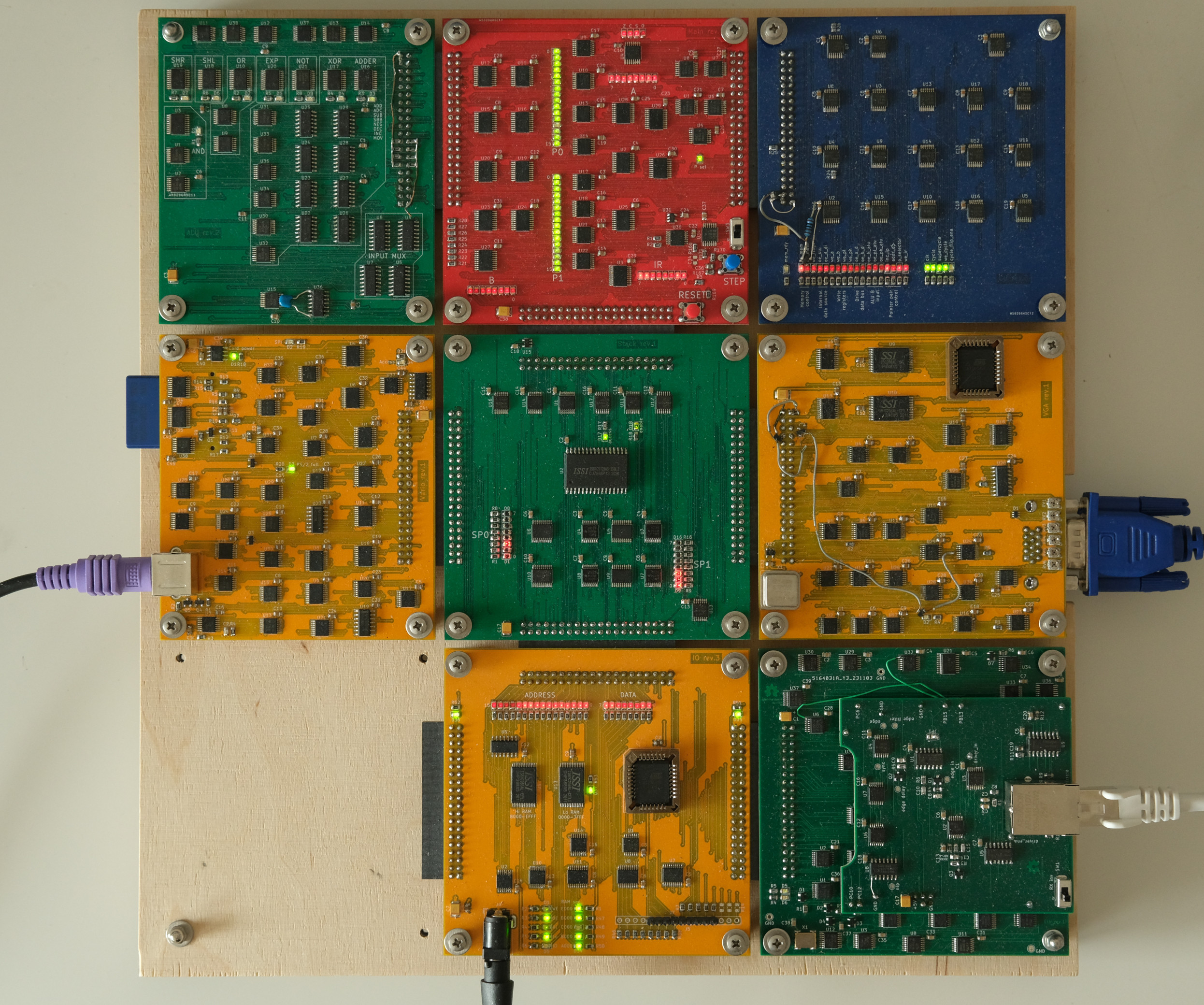 Complete computer. The new module is bottom-right.
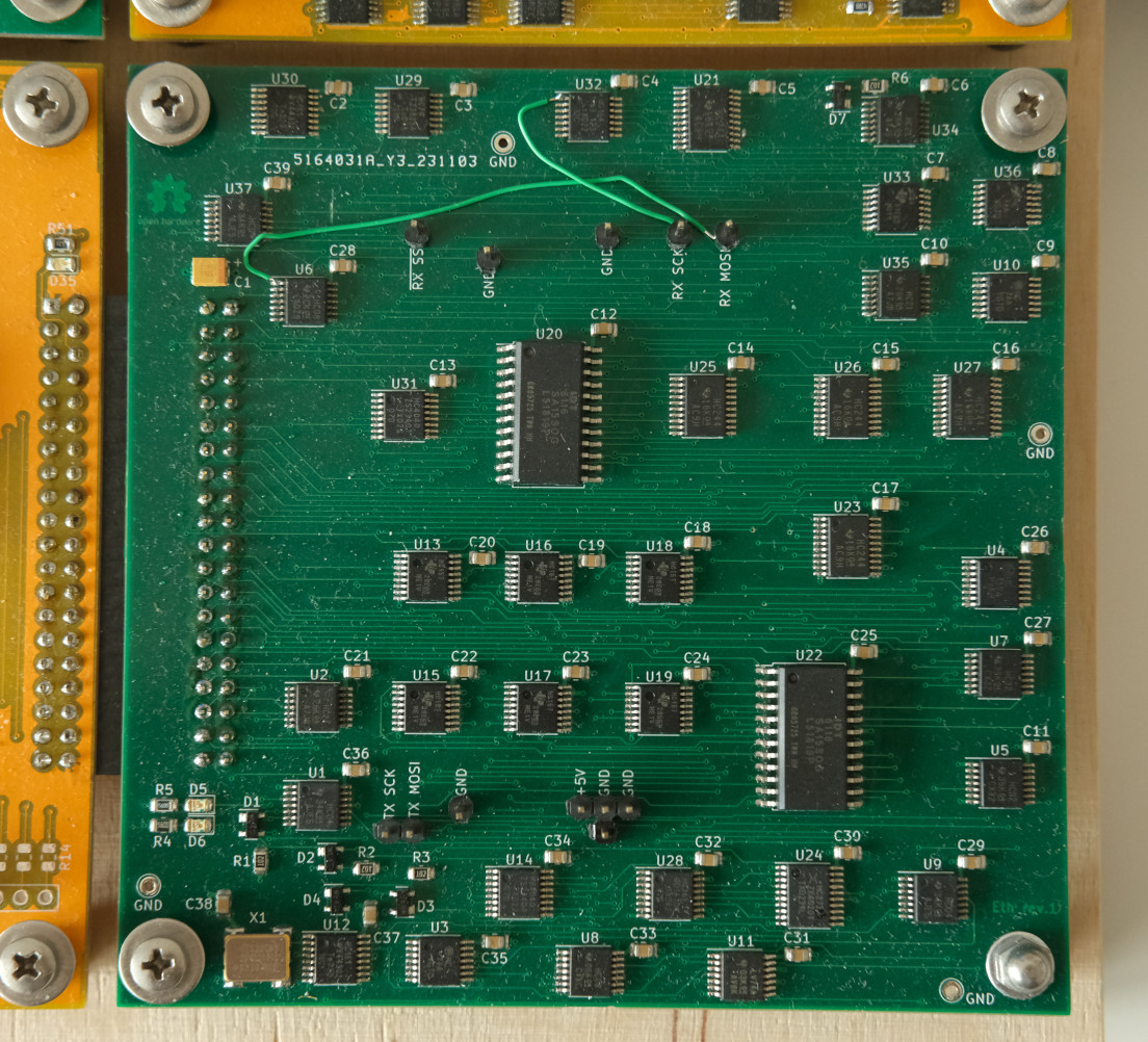 The new module with PHY shield removed. Bodge wires fix swapped SCK and MOSI.
Receiver #
Summary of receiver operation:
- SPI serial data is converted to bytewise parallel data, byte clock is extracted;
- First 6 bytes are checked against destination MAC address criteria, unmatched frames are rejected;
- Bytes are written into a static RAM buffer;
- When a frame ends, receiver is disabled and further frames are rejected until user re-arms the receiver. Byte counter is stopped, its value is made accessible to the user.
FCS is not checked in hardware.
Data collection #
Firstly, serial SPI data needs to be converted into a stream of bytes.
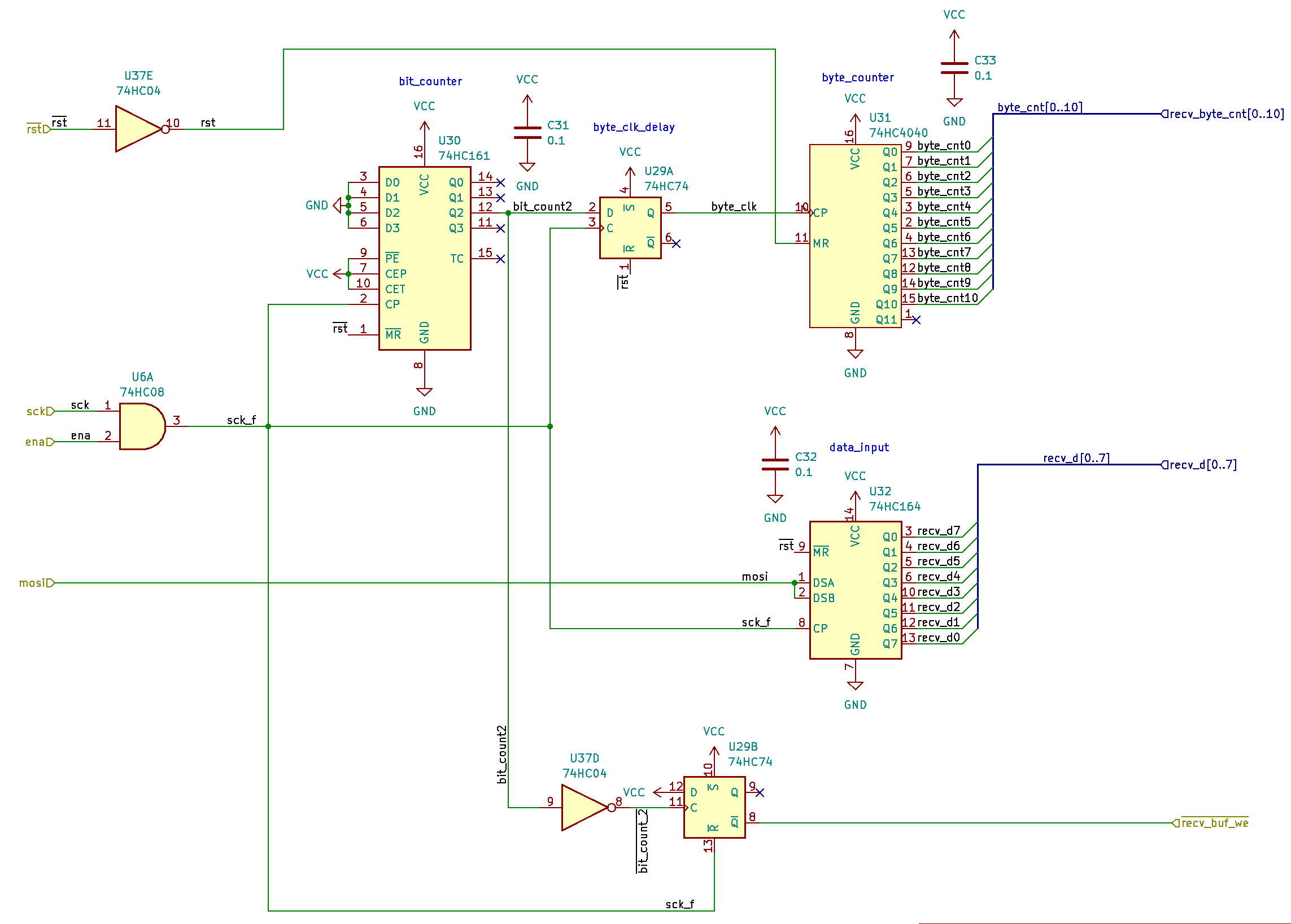
Serial data is shifted into a shift register (U32). U30 and U31 count bits and bytes respectively. Static RAM write signal recv_buf_we is formed using a D flip-flop U29B. This signal briefly becomes low after each 8 bits of input data:

Received bytes are written into a 2 kB static RAM buffer 6116 (U20).
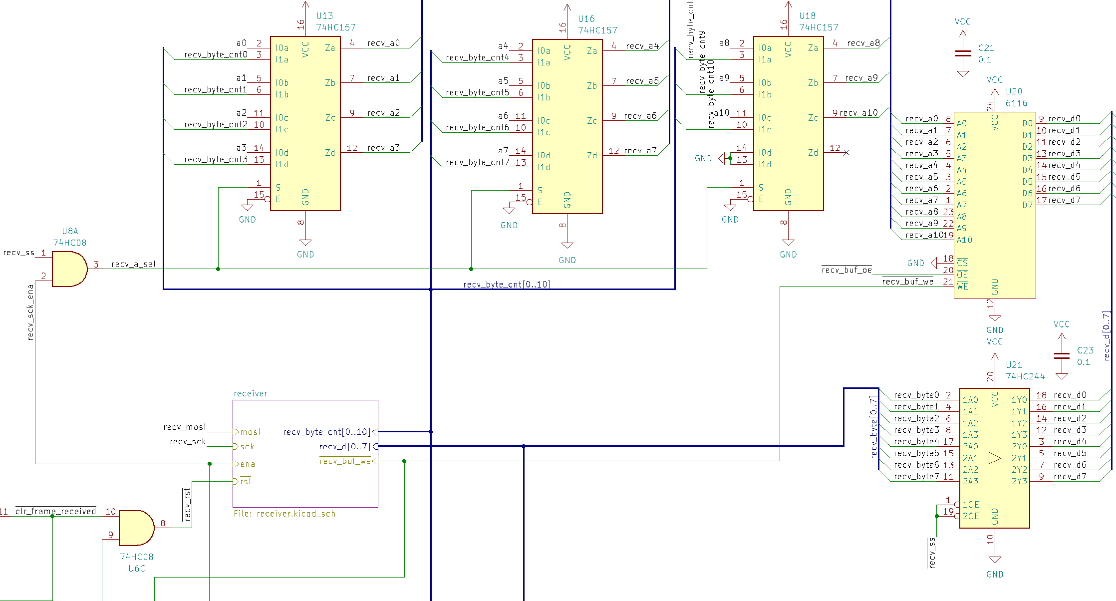
U13, U16 and U18 form an address multiplexer: it chooses either byte counter or system address bus as an address input for the SRAM (U20). A tri-state buffer U21 forwards the received byte into the RAM.
To access the received data and its length, RAM and byte counter are connected to the system data bus with tri-state buffers:
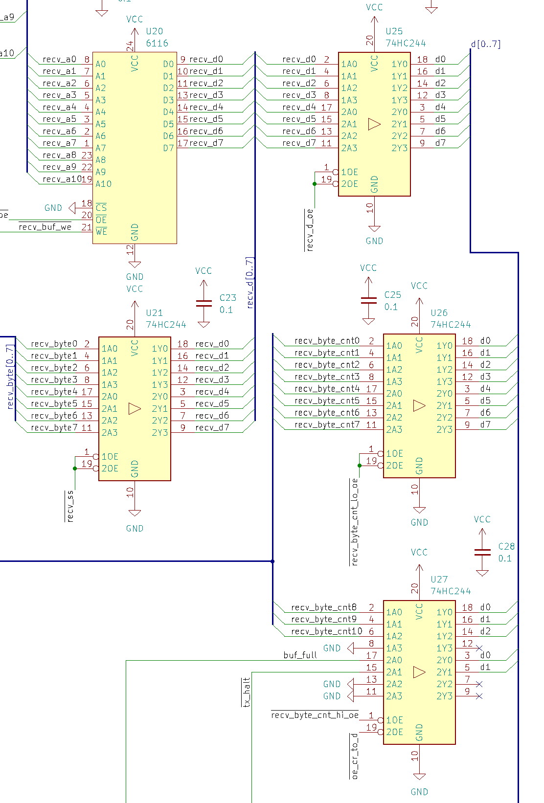
U25 connects the receiver RAM with the system data bus. After a frame is complete, the byte counter is not reset and its value is kept on the recv_byte_cnt bus. This bus is connected with the system data bus using U26 and U27. They are activated when CPU makes a read request to specific addresses. The other half of U27 makes a two-bit read-only status register which is used to query receiver and transmitter status.
MAC address filtering #
When analyzing the Ethernet traffic I noticed that frames usually come in small groups (3-4 frames together separated by a short delay). Frames in one group usually have different destination MAC addresses. This made me think that my computer won’t be able to filter received frames by MAC and re-arm the receiver fast enough to catch the frames meant for itself. I needed a hardware MAC address filtering.
Storing a custom MAC address somewhere and then comparing first 6 received bytes against it is a no-go: too complex. I could also make it a repetition of a single byte (e.g. FE:FE:FE:FE:FE:FE), but that’s boring. To bring some variation to my MAC, I made it a function of the byte index:
- Bit 0 is fixed to 0;
- Bit 1 is fixed to 1;
- Bits 2-4 are an inversion of the byte index;
- Bits 5-7 are fixed to 1.
Using this rule, the MAC address comes out to be FE:FA:F6:F2:EE:EA. We also need to accept the broadcast MAC FF:FF:FF:FF:FF:FF to work with ARP.
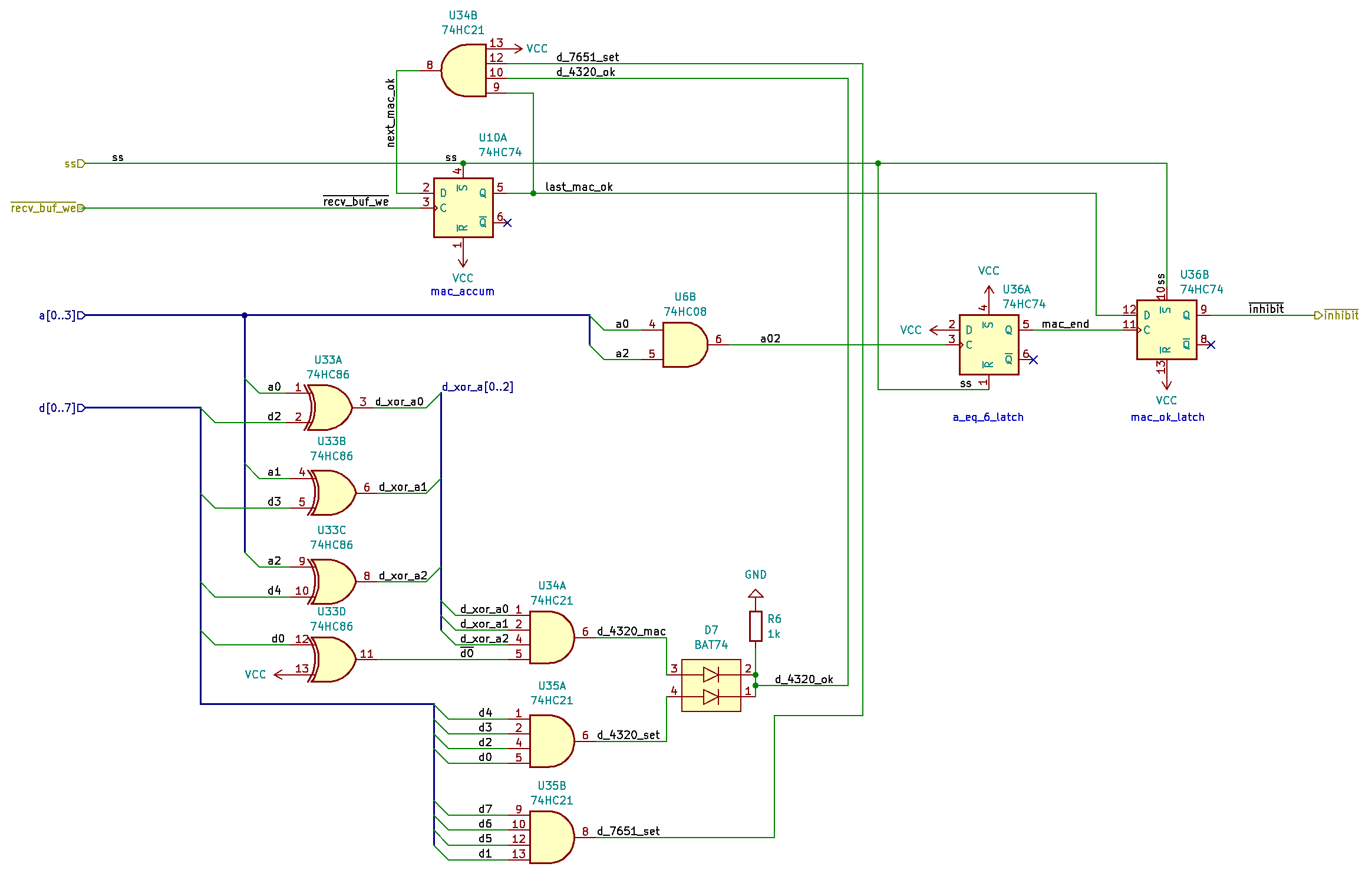
On this schematics, bus a[0..3] is the lower 4 bits of the byte counter. Bus d[0..7] is the received byte. U33 compares data bits 0 and 2-4 with their desired values, the output of U34A will be high when those bits match. U35A implements the broadcast MAC check: its output will be high when bits 0 and 2-4 are all ones. Those two signals are combined with a logical OR (implemented with diodes D7 and resistor R6). The remaining bits are checked for being all ones with U35B.
This block only checks the validity of a single byte. To check all six of them, the result is accumulated in U10A. When no frame is being received, ss (the incoming SPI slave select signal) is low and U10A is set to 1. During frame reception this value is updated for each received byte. If destination MAC address matches the criteria, the value of U10A stays high. When byte address reaches 5, the final value is latched into U36B. Its output is used to inhibit frame reception if destination address is unmatched.
Transmitter #
Similarly to the receiver, the transmitter doesn’t implement FCS generation, it is done in software. To simplify the transmitter even further, I decided to only support frames of a fixed length. This way no complex digital comparator is necessary, the frame transmission logic only depends on a single bit of the byte counter. I selected the frame length to be 1024 bytes, this is close to the usual MTU of 1500 bytes. The frame preamble (the sequence of several 0x55 ending with a 0xD5 required by 10BASE-T) is also included in those 1024 bytes and needs to be loaded there in software.
Fixing the frame length doesn’t have any effect on higher-level protocols because they encode the packet size in their headers and do not rely on the actual Ethernet frame length.
Summary of transmitter operation:
- Data is stored in a static RAM;
- 20 MHz clock is fed to a 4-bit counter, its overflow output is used as a byte clock;
- To transmit a frame, user writes to a specific write-only memory location which enables the counter;
- Parallel byte data is serialized using a shift register.
Counters #
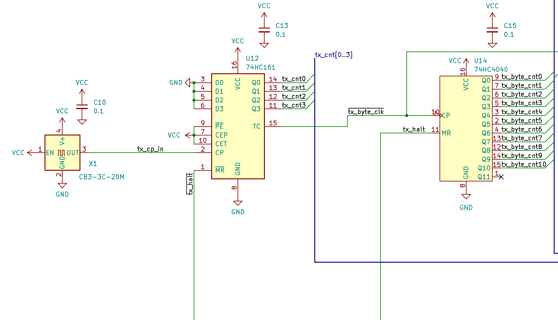
Same as in the receiver, two counters are used to count bits (U12) and bytes (U14). First counter is fed by a 20 MHz clock from an integrated oscillator. 20 MHz is not used directly, but only divided at least by 2. This way the duty cycle of the oscillator doesn’t affect the output signal.
Data flow #
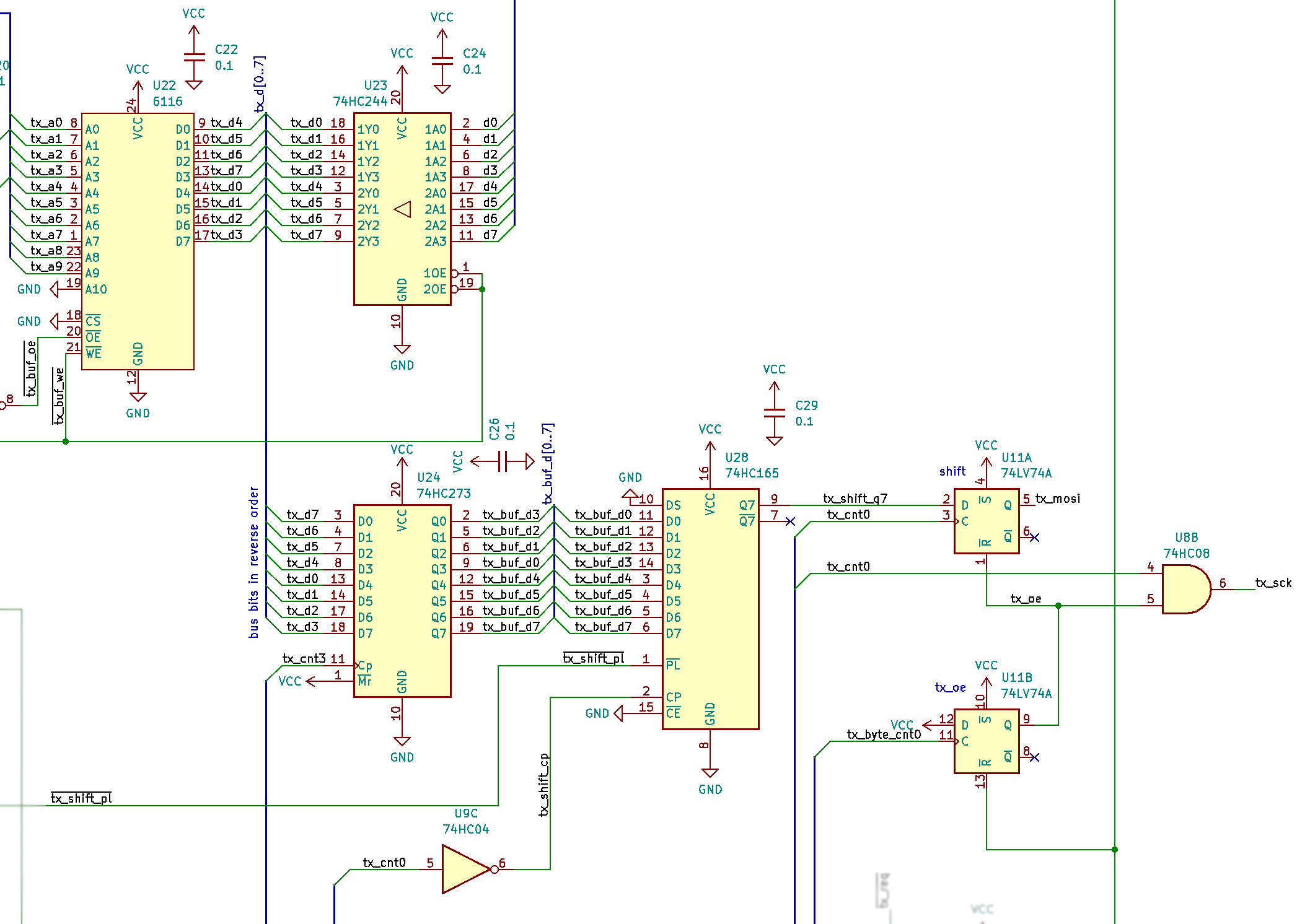
Same as in the receiver three 74HC157 multiplexors (not shown here) are used to select address input for the RAM (U22). U23 is used to load data into the RAM. U24 acts as an intermediate storage for the byte currently being transmitted. The idea here is similar to my VGA pipeline: byte counter 74HC4040 is a ripple counter and is slow to stabilize, U24 provides a stable output while RAM output is still invalid. This data is fed to the shift register U28 and shifted bit-by-bit.
After I’d built the thing I noticed that I’d messed up the order of bits coming from the RAM to the shift register. I had to shuffle bits in software to workaround this hardware bug. This was something I couldn’t test in Verilog beforehand.
To form a nice 10BASE-T signal (see my previous post) MOSI and SCK should be precisely synchronized. U11A and U8B achieve that. tx_cnt0 (bit 0 of the bit counter, 20 MHz divided by 2) is used as a clock. U11A changes its output in sync with this signal. U8B delays the clock to match the delay introduced by U11A. Because a D-latch is more complex than a simple AND gate and has a slightly larger (by 5 ns) delay, a faster 74LV74A is used here. Its propagation delay is the same as of 74HC08. This is the only chip of a “fast” family on this board.
CPU interface #
From the programmer’s point of view, my Ethernet adapter has following interface:
- Both frame buffers are mapped at
0xF000. - There are two read-only registers:
- 8-bit status register at
0xFB00has two flags:RX_FULL- a frame is received,TX_BUSY- a frame is being transmitted;
- 16-bit received data length register at
0xFB02.
- 8-bit status register at
- Writing any value at
0xFB00re-arms the receiver. - Writing any value at
0xFB01starts a transmission.
There are no interrupts since my CPU doesn’t support them.
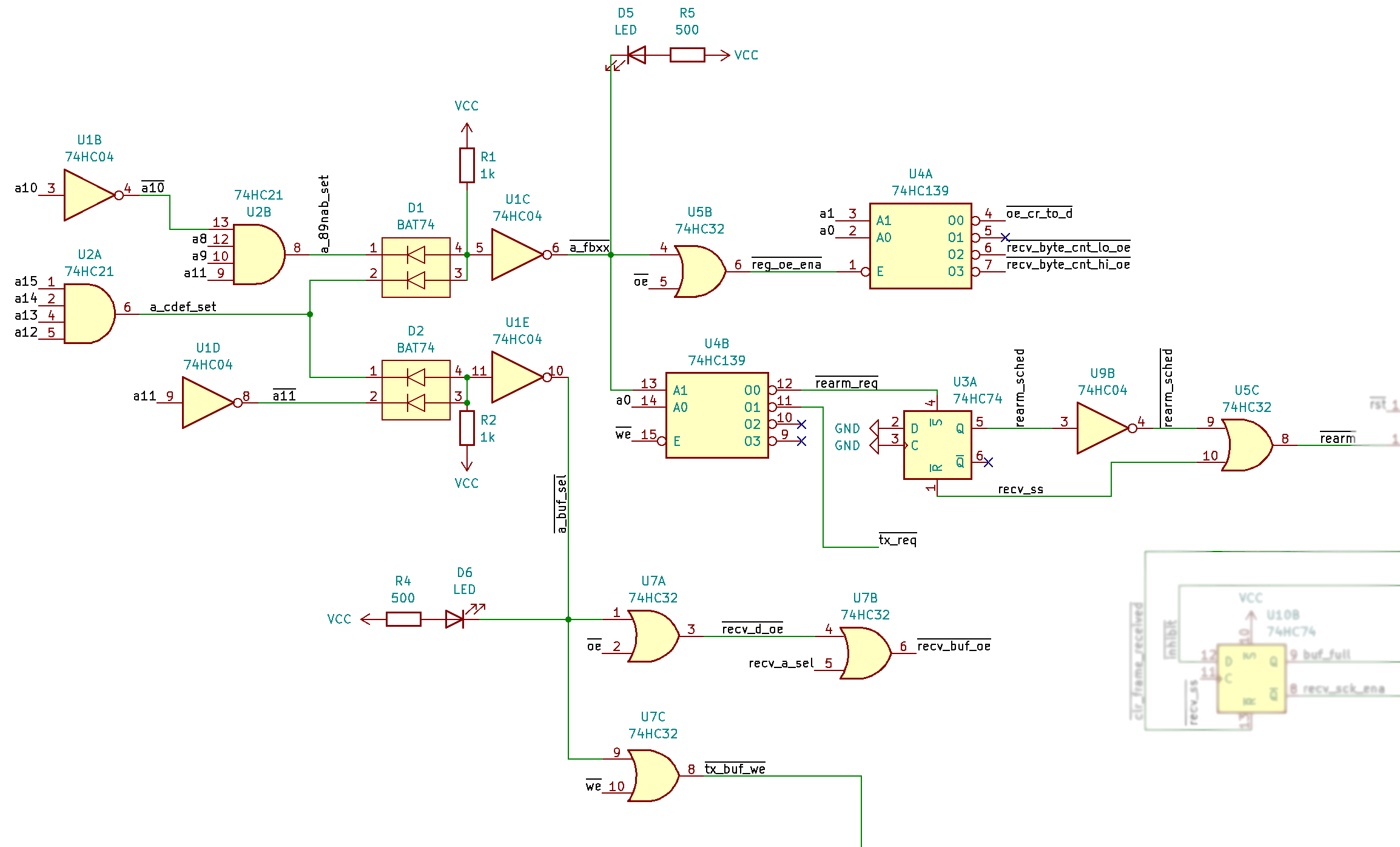
Any relevant address starts with an F (upper 4 bits are all ones). This condition is checked by U2A.
Bit 11 should be 0 for a buffer address. U1D, D2, R2 and U1E check that. Then the buffer select signal is combined with either write- or output-enable signals to select writing to the TX buffer or reading from the RX buffer.
Second hex digit being B (1011) for registers is checked by U1B and U2B. Then another diode logic block (D1, R1, U1C) combines it with the first digit check. Decoders U4A and U4B are used to select the individual function.
Two LEDs indicate buffer or register access.
Programming #
I wanted a network support for my computer, but didn’t want to implement a TCP/IP stack myself. Also I wanted a decent C compiler because my first compiler sucked and programming in assembly is annoying. So I made a C compiler. It is mature enough to compile uIP 1.0 (a tiny TCP/IP library). Despite my CPU having awfully low code density, uIP is small enough to fit into RAM and have some place left for an actual application.
Network performance is very low, but I’m still very happy with it considering that no commercial CPUs or special chips are involved here:
- Ping round trip average 85 ms;
- HTTP server download speed 2.6 kB/s (serving static files from the SD card).
Project repository #
Models, schematic files and PCB drawings are located on github.