Discrete logic IC CPU
October 11, 2020
Since I was a kid I’ve always wanted to build my own computer. First I had only vague ideas of how computers are made, then I got myself a book about building an 8080-based computer and programming it, later, of course, I’ve got a lot of experience with various computers and microcontrollers, but I’ve never built one from scratch. Now, when I’m 30, I can say I have fulfilled my childhood dream.
The main part of the project is the CPU. My CPU has 8-bit data bus width and have the address bus width of 16 bits. The CPU is attached to the peripheral module which contains program ROM, RAM, display, and keyboard.
Overview #
I wanted to make the processor as simple as possible, but not too constrained. A processor needs to do these few things:
- Read and write memory;
- Perform arithmetics;
- Have conditional and unconditional jumps.
To access memory and perform jumps you have to somehow supply memory addresses. Most of the modern processors allow user to encode direct or indirect memory address right in the load/store/jump instruction. Doing this on discrete logic would be too complicated or would require microcode. Therefore, I decided to only have indirect memory access and jumps using a pointer register. To load the registers in the first place, a load immediate instruction is necessary.
These four classes of instructions (read/write memory, arithmetics, jumps, load immediate) are the only instructions implemented.
The processor operates on 8-bit data and can address up to 65536 bytes of memory (16 bit address). This means the pointer register should hold 16 bits. From the programmer’s point of view, the pointer register P is split into two halves: PL and PH. These halves can be loaded separately. Then, the whole P register is used to access memory. Jumps are performed by swapping the P register with the instruction pointer. As a side effect, function calls can be implemented: after swapping (and jumping), P shall contain the return address.
The other two registers are named A and B. The arithmetics is performed between A and another register. There are four flags implemented:
- Z - zero;
- C - carry;
- S - sign;
- O - overflow (for signed arithmetics).
Hardware design #
Here I outline the steps taken to design the hardware.
- I thought out the overal layout of the buses and registers and sketched timing diagrams.
- Then I programmed the model in Verilog, added some test benches and ran them using Icarus Verilog.
- Time to draw the schematic diagrams! I opened the list of 7400-series integrated circuits and checked which of them could be bought in my local electronic parts store. Based on that, I selected the exact part numbers to use as registers and buffers in my project. I chose the ACT variant (or AC when ACT wasn’t available) for the best desired electrical characteristics.
- Using KiCad I started drawing schematic diagrams. At the same time I adjusted the Verilog models to match the actual schematics. This way I was sure the CPU will work as desired when I build it.
- After the schematics were ready I traced the PCBs in KiCad and ordered production from a Chinese company. At the same time I ordered the electronic components from the local retailer.
- When everything arrived, I soldered the boards.
Module layout #
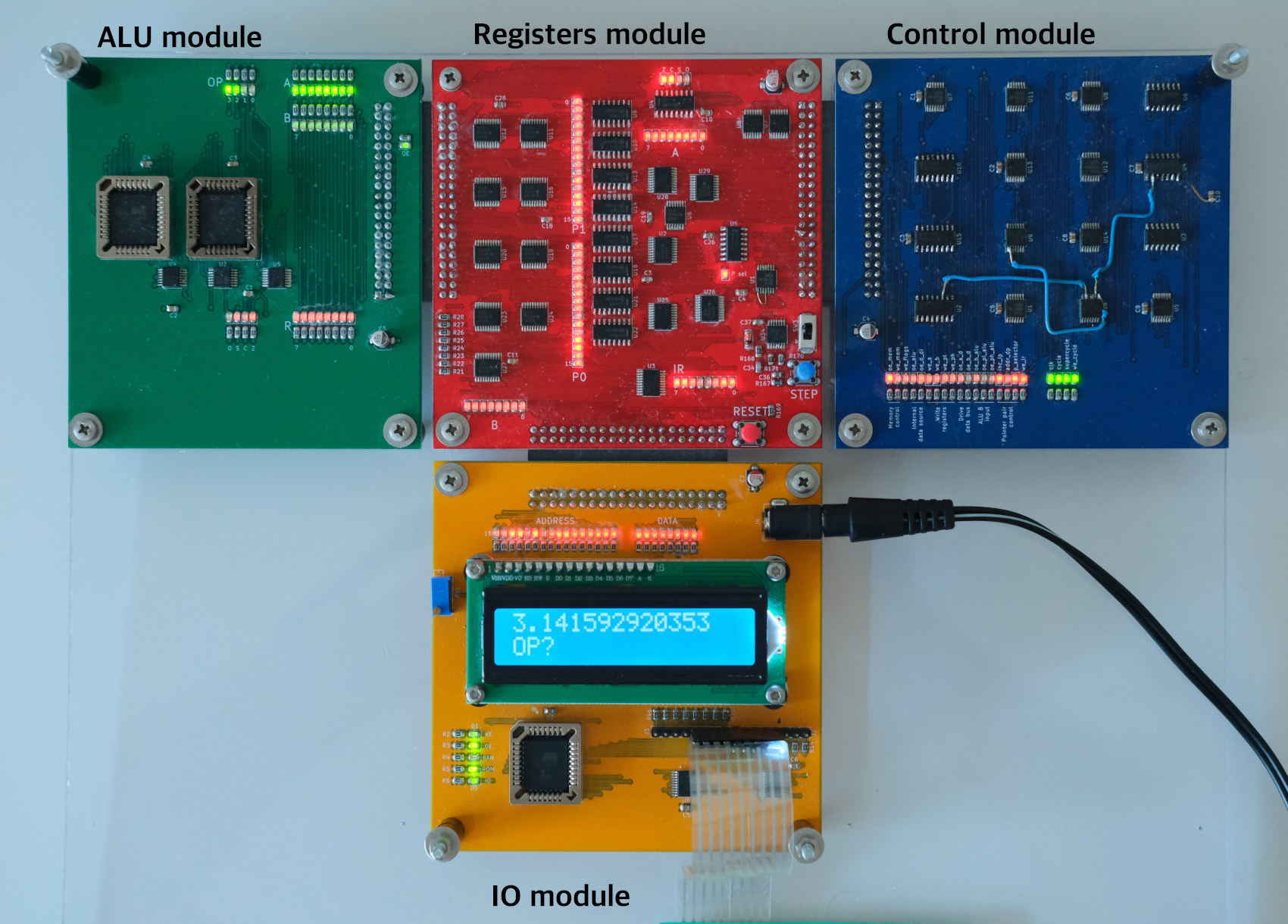
I’ve broken down the computer into four modules for two reasons. First, PCB production up to 100x100mm is much cheaper than if any dimension exceeds 100mm. Second, having separate modules makes it easier to fix hardware errors and leaves room for improvement. For example, the ALU module now is made using two ROM chips which is kind of “cheating” if you want to call the CPU discrete-logic-based.
The module layout actually helped: I have to redo the control module. The first version was ROM-based like ALU. I wanted to make it possible to reprogram the control signals and change the instruction set. But it turned out that ROM chips cannot be used as asynchronous lookup tables: during the address transition the data bus goes through random chagnes. It’s okay for the ALU because the inputs are changed on the rising clock edge and the outputs are used on the falling edge.
Registers module #

This simplified diagram shows the register layout inside the processor. Control, clock, and reset signals are not shown.
Registers A and B have one input and two tri-state outputs. Each output can be independently enabled or put into high-z state. Data input is synchronious: the value from the input bus is clocked into the register on a clock edge if the we control signal is asserted.
P is a combined register. It consists of two pairs (16 bit each) of preloadable counters. The sel input selects which pair is considered to be the instruction pointer (IP) (and can be incremented) and which one is the pointer register P. The cnt signal controls if the current IP is incremented on the clock edge. If addr_dp is asserted, the address bus is driven from the P pair, otherwise IP is used. we_dh, we_dl, oe_dh, oe_dl signals control whether the halves of the P pair are loaded or drive output bus.
As you can see on the diagram, one of the ALU inputs is always connected to the register A. The other input can be driven by any of the registers (this bus is shown in purple). If none of the oe signals is asserted, the second ALU input would be zero because of the pull-down resistors. This way arithmetics between A and zero can be performed.
Each register’s input is connected to the internal data bus (green). This bus can be driven either by ALU or by a tri-state buffer connecting it to the external data bus (red). This allows the registers to be loaded either from memory or from the arithmetic operation result.
The other outputs of registers A and B are connected to the external data bus. This way the values of these registers can be stored into RAM.
The input of the instruction register IR is connected to the data bus. This register is loaded with the current instruction on the first exectution phase. The output value of this register is used to provide control signals to everything in the processor.
Finally, the flags output from the ALU is stored into a register. Its output is then used to control conditional jumps. Additionally, the carry flag stored in the flags register is fed back to the ALU to perform arithmetics with carry.
ALU #
The ALU provides 16 arithmetic operations. I’ve decided to implement the ALU using a ROM-based lookup table. The straightforward approach would be to use one large ROM chip, feed everything to it and read the result from the output:

The following inputs are needed:
- Operands A and B (16 bits in total);
- Opcode (4 bit);
- Stored carry (1 bit);
- Invert bit - to be able to reorder input.
The output would be:
- The result (8 bits)
- Flags (4 bits)
In total, the ROM should have 22 bit input and 12 bit output. The output, of course, can be easily split into two chips, but still a 22 bit parallel ROM is pretty expensive and hard to find.
Considering all of this, I decided to process two 4-bit nibbles separately:

This way operations like addition, subtraction, bit shifts can’t be done without communication between the nibbles. I added one feedback line going from lower nibble’s output to the high nibble’s input (shown in green) and the other way around (red). To prevent feedback oscillations, logic gates were added: only one feedback line is activated at a time and selected by bit 3 of the opcode. This means operations like addition or left shift (when an information bit should go “up”) can be encoded by opcodes from 0 to 7, and operations like right shift should occupy opcodes from 8 to 15.
The overflow flag (for signed arithmetics) is taken from the upper nibble table: only higher bits influence this flag.
The carry flag is combined from both parts by a NAND gate. This way carry can be set by either of tables.
The zero flag is calculated by a logical NOR of all the output bits. This way, Z will be set if R is zero.
Finally, the sign flag is just the upper bit of the result.
These tables fitted nicely into two cheap 28C256 32k x 8bit ROM chips.
For convenience, processor needs a MOV instruction to copy one register’s value into another. With the selected architecture, it can only be done via ALU. To make this instruction usable, it shouldn’t modify flags. To assure this, additional control logic was added which stores flags only if the ALU opcode is not MOV.
Instruction encoding #
All instructions except for LDI are encoded in one byte. LDI is coded in two bytes: the second byte is the immediate value.
In the control unit the following circuit decodes the instruction opcode stored in the instruction register:
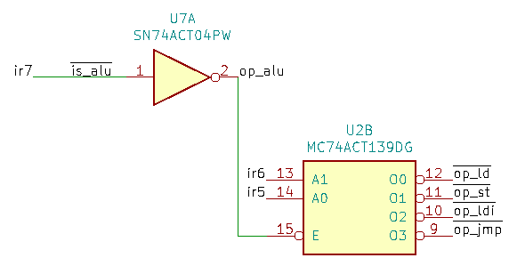
Signals ir7, ir6 and ir5 are the three upper bits of the IR. When bit 7 is low, op_alu is high indicating an ALU instruction. If bit 7 is high, the decoder U2B is enabled and the other two bits are used to select one of the four remaining instructions.
ALU instructions #
One operand for this instruction is always A, the other one is encoded in the last two bits:
0ooooidd
 \__/|\/
   | | -- other register operand (00 - zero, 01 - B, 10 - PL, 11 - PH)
   | +--- inversion bit (0 - "SUB A, B", 1 - "SUB B, A")
   +----- ALU operation
Example: SUB PL, A would be 00001110 (SUB opcode is 0001).
LD instruction #
100???rr
      \/
       -- register operand (00 - A, 01 - B, 10 - PL, 11 - PH)
Example: LD PH would be 10000011.
ST instruction #
Only A or B can be stored into memory. Storing PL or PH doesn’t make sense anyway: they contain the address of the memory location.
101????r
       |
       -- register operand (0 - A, 1 - B)
Example: ST B would be 10100001.
LDI instruction #
110???rr bbbbbbbb
      \/ \______/
       \     +---- immediate value
       |
       +---------- register operand, same as for LD
Example: LDI PL, 0xF0 would be 11000010 11110000.
Jump instructions #
111?ciff
    ||\/
    || -- flag (00 - Z, 01 - C, 10 - S, 11 - O)
    |+--- inversed condition (0 - selected flag should be 1, 1 - selected flag should be 0)
    +---- flag selection disabled (0 - a flag is selected, 1 - condition result is always 1)
Examples:
JMP:11101000NOP:11111111JNS:11100110
Instruction execution #
On the control board instruction execution is encoded with discrete logic. Using the value of the instruction register (IR), clock, and flags, the control signals for the registers, ALU, and memory are calculated. Such signals include (but are not limited to):
- load
IR, - increment
IP, - write or read memory,
- write any register,
- enable a register or ALU output to drive a bus.
Most of the instructions are executed in two clock cycles. The LDI (load immediate) instruction requires four cycles: IP should be incremented twice.
Using three flip-flops three additional slower clock signals are generated from the master clock (clk):
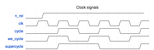
cyclecontrols the execution cycle of the instruction. Whencycleis low,IRis loaded, whencycleis high, the instruction is executed.we_cycleis basicallycyclephase-shifted by 90°. It’s used to generate then_we_mem(write memory) signal for theSTinstruction.supercycleis only active when the longLDIinstruction is executed.
The general rules of the control signals:
- Data is latched and IP is incremented on falling clock edge;
- Control signals change on raising clock edge.
These rules assure that values on the buses (ALU output, memory output) are stable when registers are latched.
Load register from RAM (LD)
#
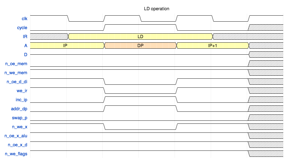
- RAM is always set in read mode (
n_mem_oelow,n_mem_wehi) - ALU output is disabled
- Registers output to external data bus is disabled
- During the second phase (
cycleis high):Pdrives the address bus (addr_dpis high),IPis incremented (inc_ipis high),IRis not latched (we_iris low),- Register selected by opcode is latched (
n_we_xis low).
Store register to RAM (ST)
#
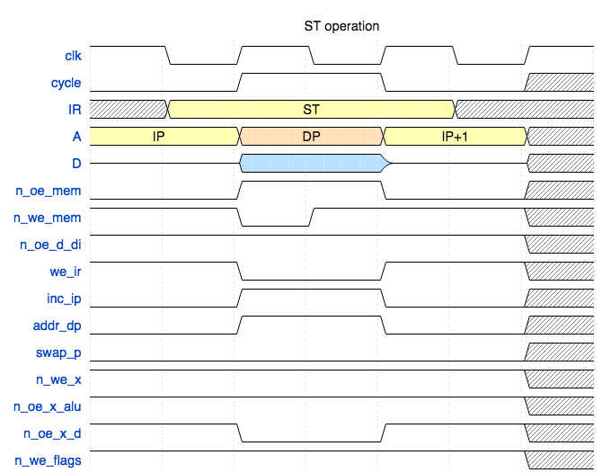
This instruction is similar to LD, but the write signals are formed on the data bus. During the second phase n_mem_oe is set to high which makes RAM chip release the data bus. To write the byte, n_mem_we is pulled down for the first half of the second phase. The data is written into RAM when this signal goes up. This happens on falling clock edge when the data is stable.
Arithmetic instructions #
There are two types of instructions involving ALU: direct and inversed. In the direct case the operation result is written into A, in the inversed case the ALU inputs are flipped and the result is written into the other register (not A). For example, SUB A, B is a direct instruction and SUB PL, A is inversed. In the second case PL will be modified.
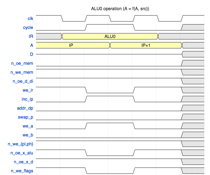
I’m only showing here the direct ALU waveform. The other one can be found in the repository.
Load immediate value (LDI)
#
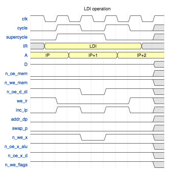
This is the most complex instruction. It takes four clock cycles. IP is incremented two times. After the first increment the byte from the data bus is latched into the selected register.
The timing diagrams are drawn with Wavedrom.
Peripheral board #
The peripheral board provides 32k ROM, 28k RAM and minimum IO: a keyboard and a display. The memory is mapped as follows:
0x0000 - 0x7FFF- ROM0x8000 - 0xEFFF- RAM0xF000- keyboard (write column mask, read row mask)0xF002- LCD module control (write only)0xF003- LCD module data (write only)
A matrix keyboard interface is implemented using an 8-bit register to store the column mask and a 3-state 8-bit buffer to drive the data bus with the row mask. Keyboards up to 8x8 are possible, but I could only find and buy a 4x4 matrix keyboard.
A common 16x2 LCD module is used as a display. Its 8 bit interface bus perfectly matches CPU buses with minimal extra logic.
Programming in assembly #
Given all the limitations of the processor, programming it in assembly is a pretty challenging task.
Functions #
When a jump is performed, IP an P are swapped. This way jumps can also be viewed as function calls: the return address will be stored in P on function entry. We just need to save it in a variable.
function:
    mov a, ph               ; arithmetics (including MOV) is only possible between A and other register
    mov b, a
    mov a, pl
    ldi ph, hi(ret_addr)
    ldi pl, lo(ret_addr)
    st a                    ; low byte of the return address is stored first
    inc pl                  ; ret_addr is aligned, overflow over 256 doesn't happen
    st b

    ; ... function body

    ldi ph, hi(ret_addr)
    ldi pl, lo(ret_addr)
    ld a
    inc pl
    ld ph                   ; ph can be loaded directly
    mov pl, a
    jmp                     ; return from the function

    ; in data section:
    .align 2
ret_addr: res 2
Since ret_addr is statically allocated, this function cannot be re-entered. And if you call other functions from this one, they should use distinct variables to store return addresses. If you need recursion, you have to implement a software stack.
The trick with alignment helps to avoid overflows and save code bytes when loading/storing the second byte of a word. With no alignment, we would need either to increment PH if carry is set or load PH and PL the second time:
function:
    mov a, ph
    mov b, a
    mov a, pl
    ldi ph, hi(ret_addr)
    ldi pl, lo(ret_addr)
    st a
    mov a, 0                ; Arithmetics between A and 0 is allowed
    inc pl
    adc ph, a
    st b
Parameter passing #
Even a single byte parameter can’t be passed in a register: all the registers are used to save the return address. The best way to pass a function parameter is to have a static variable for it. Most of the functions aren’t recursive anyway.
High-level language #
After I got everything working, I wanted to have a (relatively) high-level language compiler for my processor. At first I found an ancient C compiler from 1980s: SmallC-85. It targets Intel 8080 which is pretty close to what’s desired (8 bit data, 16 bit address). Changing the backend was pretty easy, but there was a problem: SmallC-85 uses stack extensively. For example, a simple line like a = b + c; would compile into something like this (pseudo-assembly):
push b
push c
pop r1
pop r2
add r1, r2
push r1
pop a
With a software stack this approach is totally unacceptable.
Then I tried to make my own LLVM backend, but I found myself overwhelmed by the complexity of the task and procrastinating and gave up.
Natrix #
Finally, I decided to make my own compiler from scratch. I used the Lark parsing toolkit for Python and implemented a C-like language which I called Natrix after a snake.
Basically, Natrix came out to be almost a subset of C. What makes it different is the lack of stack allocations. All local variables are static (the names are mangled so that there’s no name collision between functions). Function parameters and return values are transferred in static variables too.
Inside one translation unit a call graph is built, and if recursion is detected, recursive calls are done via software stack: all local variables are pushed onto stack before the call and restored afterwards.
Internal temporary variables (also static) are introduced to store intermediate results in calculating expressions. These variables are never stored on stack.
These limitations with functions lead to another limitation: a function call result can only be assigned to a variable. You cannot use a function in an expression. Otherwise, each function would have to use its own set of temp variables.
The other difference with C is the lack of static casts. In C narrow types are implicitly cast to int, then the operation result is cast back if assigned to a variable of a different type. In Natrix there are no implicit casts. Calculations are performed in the explicitly specified type. This helps to reduce unnecessary overhead and make it clear for the programmer which type is currenly used.
Applications #
These are the two applications I made for the computer.
The soft floating point calculator can perform four arithmetic operations. The numbers are coded by 16 bytes (14 bytes for 14 decimal digits of mantissa, 1 byte for the exponent and 1 sign byte). You can see how slow it divides two numbers.
In the maze game you have a 1d view on a 2d maze and must find a key and then a door to the next, bigger, level. You look at one row of the maze at the time, but you can rotate your view. The game is written in Natrix.
Project repository #
If you are interested, you can find the project repository here on GitHub.