Building a new discrete logic ALU
February 16, 2021
After a long delay I have continued my discrete logic computer project. Last time I had a working system, but the ALU was based on two ROM chips, which wasn’t nice. It’s time to change that.
The ALU #
The ALU is asynchronous, it takes two 8-bit values, a carry flag and an operation code as an input and produces an 8-bit result and 4 flags. It can also set the output to High-Z state and flip the inputs. Here’s what the old ALU looked like:

I didn’t want to modify anything else but the ALU, so I had to support exatly the same interface.
Overall architecture #

To support inputs flipping, the inputs are fed to a multiplexer (MUX). The multiplexer’s two outputs are then fed to all operation blocks (OP1-OPn). Each block has a three-state output. All of them are directly connected to the output bus. This way the whole ALU output can be High-Z if none of the blocks are selected.
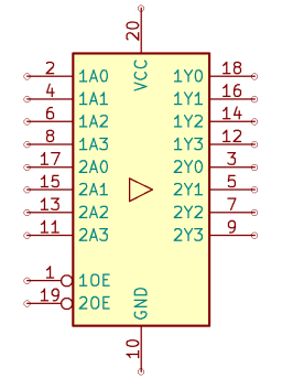
The buffer 74AC244 is used as a final stage of each operation block. It’s a three-state buffer which either drives the output bus with its input value or stays in a High-Z state. Here’s what its symbol looks like:
Now we need to design the individual operations.
Operations #
These are the operations supported by the ALU:
MOV- copy a value;ADC,ADD- addition (with and without carry);SBB,SUB- subtraction (with and without carry);INC,DEC- increment and decrement;NEG- negation;NOT- bitwise inversion;SHL,SHR,SAR- bit shifts by one bit;AND,OR,XOR- bitwise boolean operations;EXP- expand carry to all bits of the result.
Simple operations #
EXP can be done by simply feeding the carry to all inputs of the corresponding 74AC244.
SHL, SHR and SAR are simple too. Since we only shify by one bit, we need to feed the shifted input to the input of a buffer chip.
For NOT we can take a different chip: 74AC240. It works the same as -244, but inverts the inputs.
For AND and OR we simply lead the inputs through a chip (74AC08 for AND, 74AC32 for OR) and feed the result to a -244 buffer.
Designing an adder #
So far 7 out of 16 operations are implemented. We can notice that the rest (expect for XOR) can be expressed via addition or subtraction:
ADD A, B = A + BADC A, B = A + B + cSUB A, B = A - BSBB A, B = A - B - cINC A = A + 1DEC A = A - 1NEG A = 0 - AMOV A, B = B + 0
Here A and B are 8-bit operands and c is a 1-bit carry flag. To support these operations, a universal adder must implement the following functionality:
- Add or subtract;
- Add carry bit to the second operand;
- Use zero instead of either operand;
- Swap operands;
- Use one as a second operand.
Swapping of the operands is already implemented by the input multiplexer. We just need to add a XOR gate so that we can swap depending on both the input invert signal and on the internal condition.
Disabling either of the operands is implemented by the multiplexer too. The multiplexer chips 74AC157 have an “enable” flag, which can be used to set their outputs to all zeroes.
To use one as a second operand, we can set it to zero and then set the lowest bit to one. This can be done with one extra OR gate.
So far so good. Now let’s design the adder itself.
Here’s a full adder:
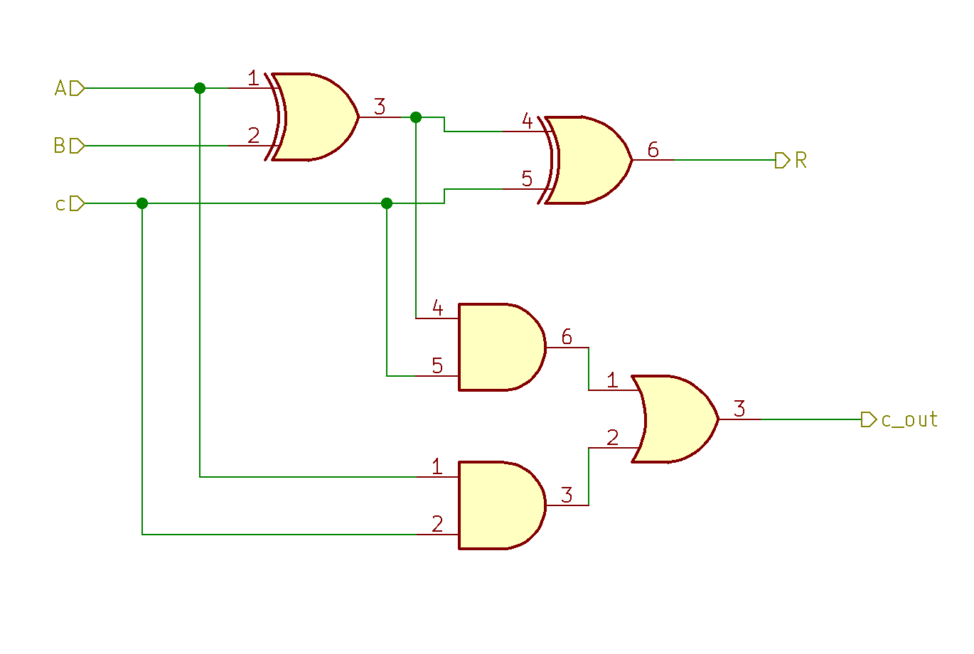
It has three inputs, A, B and c, and two ouputs, R (the lower bit) and c_out (the upper bit). Here’s the adder’s truth table:
A   B   c  |  R  c_out
0   0   0  |  0  0
0   1   0  |  1  0
1   0   0  |  1  0
1   1   0  |  0  1
0   0   1  |  1  0
0   1   1  |  0  1
1   0   1  |  0  1
1   1   1  |  1  1
The adder implements the formula A + B + c. What if we want to subtract? The formula would be A - B - c and the corresponding truth table is:
A   B   c  |  R  c_out
0   0   0  |  0  0
0   1   0  |  1  1
1   0   0  |  1  0
1   1   0  |  0  0
0   0   1  |  1  1
0   1   1  |  0  1
1   0   1  |  0  0
1   1   1  |  1  1
We can see that the R output is the same for both adder and subtractor, but c_out is different. To change an adder into a subtractor we need to add two invertors:
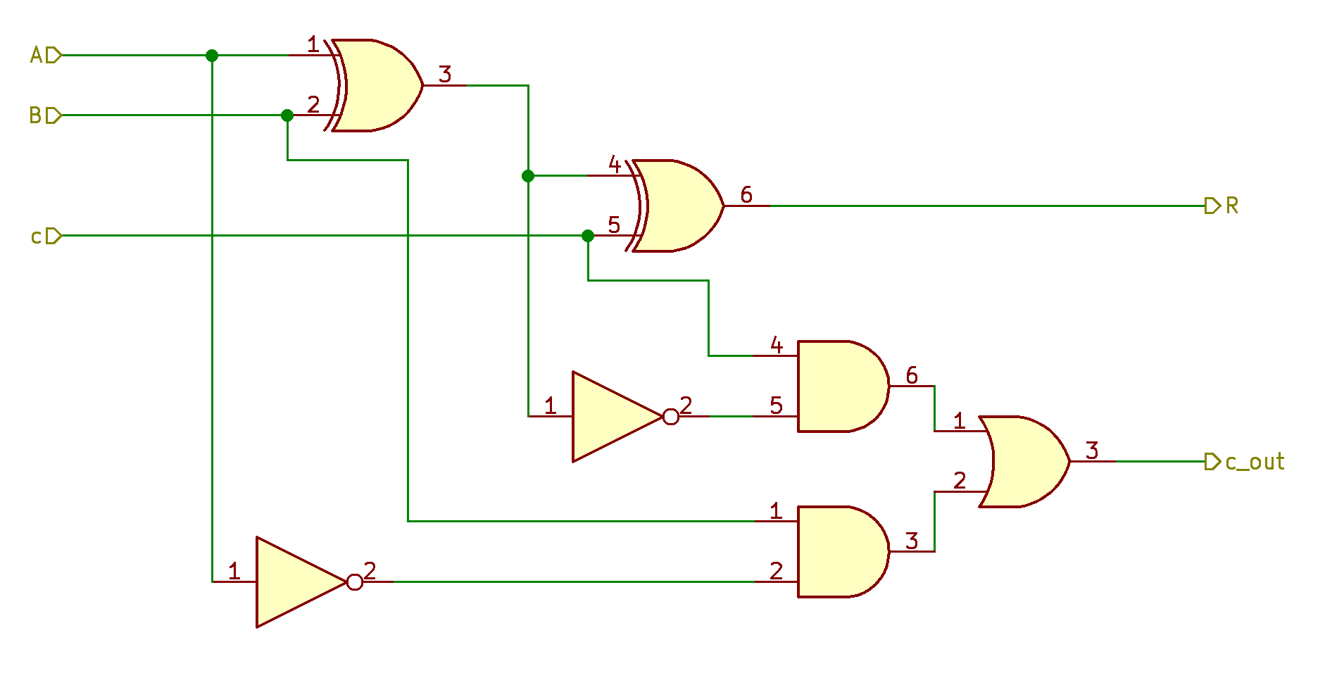
But we need this circuit to switch from an adder to a subtractor on demand. We need controlled invertors which can invert on demand. Controlled invertors are XOR gates:
Looks good. Now, if sub is one, addition becomes subtraction. Other good news is that we can get XOR of A and B for free!
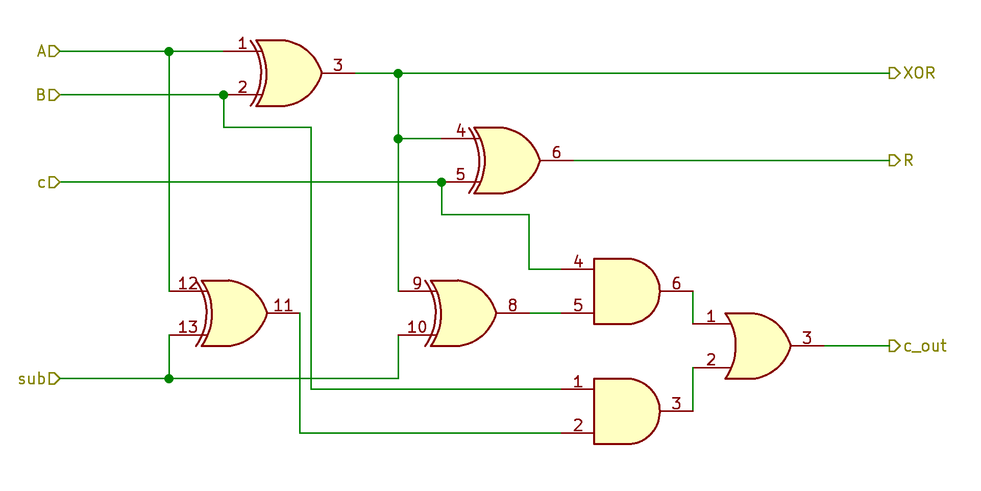
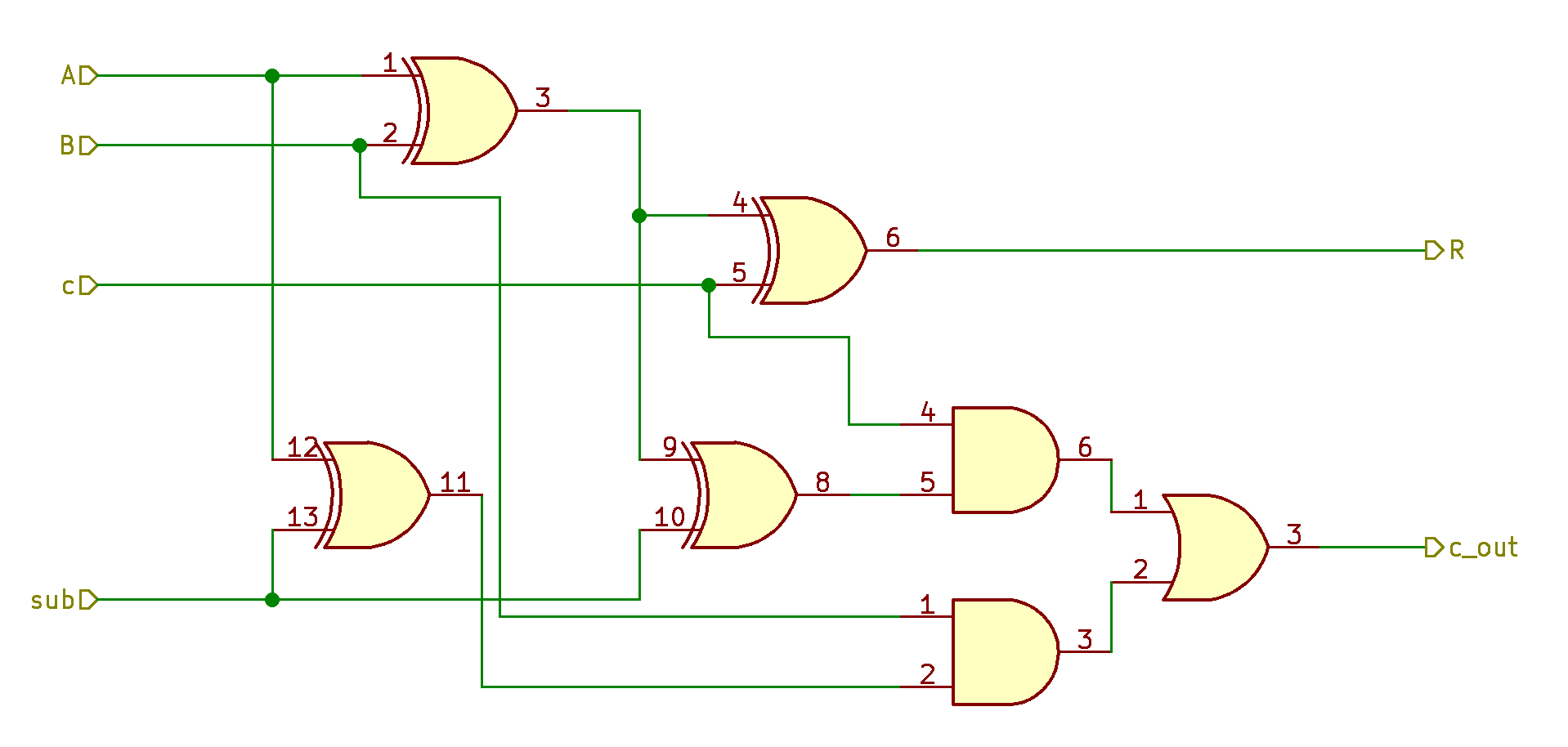
Now we have all the remaining operations with a signle universal block. It’s a technical matter to connect eight single bit adder blocks in a ripple-carry chain and implement the logic to drive all the control signals depending on the ALU operation code.
The result #
Here’s what the assembled ALU looks like.
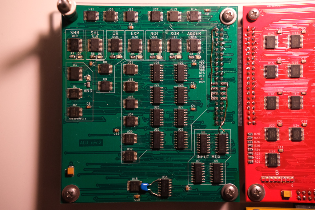
The blue capacitor is there to prevent high-frequency noise which happened sometimes and messed everything up. I found out the location of the capacitor by randomly touching the board. When I touched the right spot, noise disappeared, so I soldered there a capacitor.
And I have raised the CPU frequency to 1.75 MHz. Now it runs much smoother: division doesn’t take noticable time, the maze game also doesn’t feel slow to play. I think the old ALU would work at the raised frequency too, so it’s an unrelated change. But still cool.